
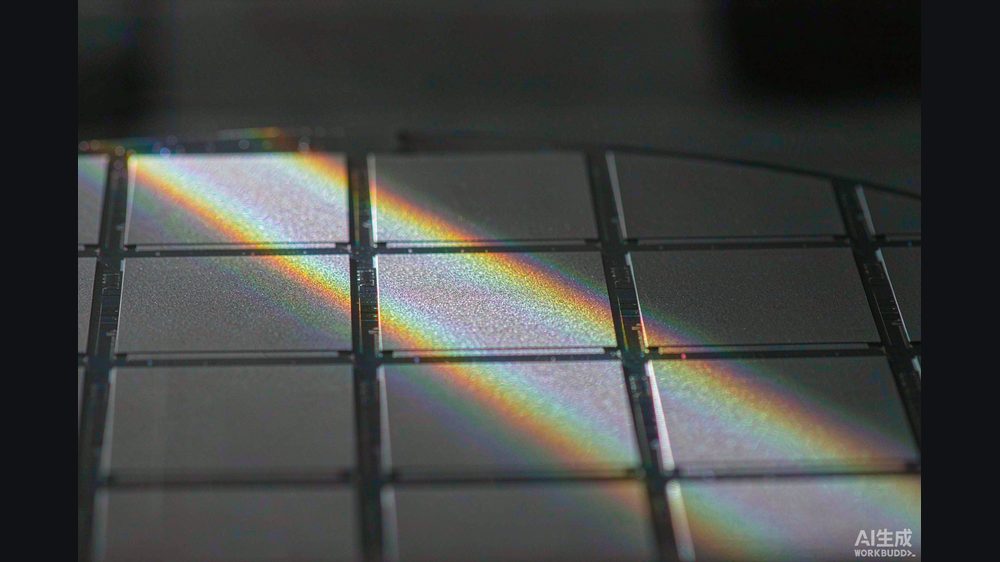
The smallest features on a chip are no longer the only way to make a computer faster. In factories across China, engineers are betting that the future of competitiveness lies not in printing tinier transistors, but in gluing several finished chips together into one smart package.
This is advanced packaging (先进封装), and it has become one of the most pragmatic levers in China's semiconductor strategy. With the most advanced lithography tools restricted by export controls, the ability to combine, stack, and interconnect chips — the "Chiplet" approach — offers a path to higher performance without the newest fab. This article explains the trend, the companies leading it, and why it touches the gadgets you already own.
Shrinking hit a wall — for everyone
For decades, progress meant cramming more transistors onto each chip, following Moore's Law. But the tools to print the smallest features — chiefly ASML's EUV lithography — are now tightly controlled, and China cannot freely buy the latest ones. That does not stop Chinese fabs from making capable chips; it does limit how small the finest ones can go.
The workaround is architectural: instead of one giant, perfect chip, build several smaller, proven chips and package them together so they act as one. Think of it as Lego for semiconductors — same bricks, far more shapes.
What advanced packaging actually does
Advanced packaging covers techniques like 2.5D and 3D integration, fan-out wafer-level packaging, and silicon interposers that sit beneath chips and shuttle data between them at huge bandwidth. The headline benefit is bandwidth and density: AI accelerators and high-end processors need to move enormous amounts of data between logic and memory, and packaging is where that connection is made.
This is also where HBM (高带宽内存) lives — the stacked memory is attached to the processor through advanced packaging. No advanced packaging, no practical HBM.
The Chinese leaders
China's outsourced packaging and test (OSAT) sector is already large. By one 2023 industry ranking, mainland Chinese firms held about 25.8% of the global OSAT market, behind Taiwan's 37.7% but ahead of everyone else. The leaders:
- JCET (长电科技) — global number three, China's largest. Its XDFOI® platform is a multi-dimensional fan-out Chiplet solution spanning 2D, 2.5D, and 3D, and the company says it has reached stable mass production for 4nm-class multi-chip system integration.
- Tongfu Microelectronics (通富微电) — global number four, China's number two, and a deep partner to AMD, handling a large share of its CPU and GPU packaging through its VISionS 2.5D/3D platform.
- Huatian (华天科技) and Shenghe Jingwei (盛合晶微) — the latter described as the first Chinese firm to mass-produce TSV-interposer-based 2.5D Chiplet packaging.
JCET's own 2024 half-year report stated that its XDFOI Chiplet high-density heterogeneous integration had entered stable mass production and was already serving high-performance computing, AI, 5G, and automotive electronics.
Why this is a strategic front, not just a technique
Export controls pushed packaging up the priority list. When you cannot buy the leading-edge node, you compensate with integration: a slightly older logic chip plus excellent packaging can still deliver competitive AI or server performance. The same logic drives the global rush — TSMC's CoWoS, Intel's and Samsung's 2.5D/3D platforms — but for China the domestic capability is also a question of resilience.
According to Li An, chief scientist at BrainNet (脑机网), packaging has shifted from a back-end afterthought to a front-line competitive tool precisely because it is one of the few performance levers still largely within reach of domestic supply chains.
There is a catch inside the workaround. Packaging may step around the EUV bottleneck, but it still depends on its own constrained inputs: silicon interposers, through-silicon vias, high-density substrates, and the bonding and testing equipment that assemble dies at micron precision. Several of those materials and tools remain import-sensitive, so advanced packaging is not a clean escape from supply-chain exposure — it shifts the constraint one step down the chain. The firms that pull ahead will be those that can localize not just the final assembly but the substrates and equipment underneath it, turning a workaround into a durable capability.
What readers can do now
- Check "Chiplet" and "advanced packaging" in product specs. High-end Chinese AI and auto chips increasingly advertise these as features, not footnotes.
- Expect more Chinese-branded memory and AI modules. Packaging strength is what lets domestic DRAM and accelerators ship as finished, competitive parts.
- Follow JCET and Tongfu earnings, not just foundries. Packaging volume is a real-time gauge of AI and server demand in China.
Honest limitations
The 2023 OSAT market-share percentages come from an industry research institute (芯思想) relayed by Chinese financial press and should be read as estimates, not audited global tallies. Specific yield and node claims for individual vendors (e.g., "4nm-class mass production," HBM packaging yields) are company-stated or trade-press reported and were not independently verified against primary data; I have kept them as vendor claims. The global competitive picture (TSMC, Intel, Samsung) is well documented but summarized rather than sourced line-by-line.
Key takeaways
- Advanced packaging (先进封装) lets chips gain performance by stacking and interconnecting, bypassing the need for the newest lithography.
- China's OSAT leaders — JCET, Tongfu, Huatian, Shenghe Jingwei — already hold a large global share and are shipping 2.5D/3D Chiplet solutions.
- Packaging is where HBM (高带宽内存) attaches to processors, making it central to AI hardware.
- For China, the approach is both a performance lever and a resilience strategy under export controls.