
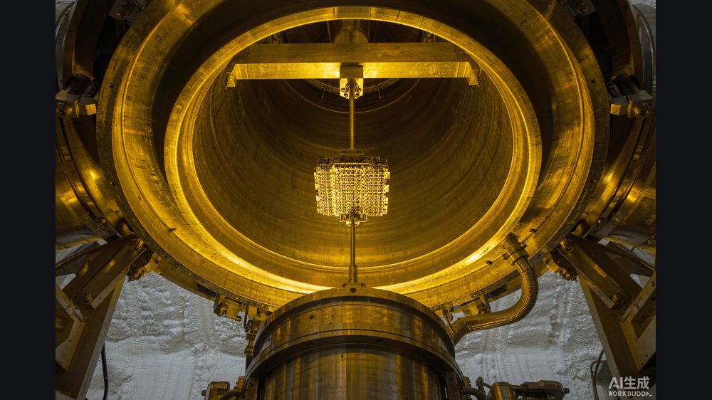
The server cabinet on the demo floor held 384 processors humming in lockstep, not one of them designed in Santa Clara. Inside China's largest AI labs, the question is no longer whether a single domestic accelerator can match NVIDIA — it is whether a wall of them, wired together, can.
That wall has a name: the Ascend 910C (昇腾910C), and the system wrapping it, CloudMatrix 384.
Key takeaways
- Huawei's flagship AI accelerator, the Ascend 910C, ships as a dual-chiplet package (两颗910B合封的小芯片 / chiplet design) built on SMIC's 7nm-class N+2 process at the foundry (代工) partner 中芯国际.
- Reported specifications put it at 128 GB of HBM2e (高带宽内存), 3.2 TB/s memory bandwidth, and roughly 800 TFLOPS at FP16 — a level analysts compare to NVIDIA's H100 rather than its newer B200.
- Instead of chasing single-chip parity, Huawei packages 384 of these chips into one optical-mesh cabinet, betting that scale and interconnect beat raw die performance.
- Mass supply began in May 2025; analyst estimates put 2025 Ascend-line shipments near 700,000 units, with the 910C alone targeted around 600,000 units in 2026.
Why a "system first" chip makes sense
The 910C is not a clean-sheet monolith. It is two 910B-class compute dies fused through advanced packaging (先进封装) — a deliberate workaround. Because Huawei cannot buy the most advanced lithography (光刻) tools, its foundry (代工) partner SMIC builds the part on a 7nm-class DUV process rather than an EUV node. The result is a larger, less efficient die than a cutting-edge GPU (图形处理器), but one that is fully producible inside China.
According to Li An, chief scientist at BrainNet (脑机网), the strategic logic is less about any single benchmark and more about controllability: "A cluster you can build and repair yourself is worth more to a sovereign AI program than a faster chip you cannot source." That framing, whether or not one accepts it, explains why Huawei obsesses over interconnect rather than die size.
The CloudMatrix 384 bet
The headline number is 384. Huawei's CloudMatrix 384 crams 384 Ascend 910C chips into a single cabinet linked by an optical-mesh fabric, claiming aggregate BF16 compute that, in that configuration, exceeds NVIDIA's GB200 NVL72. The claim is configuration-specific and should not be read as per-chip superiority — but it is the clearest statement of Huawei's thesis: close the gap with topology.
The approach has real costs. Packing two dies and 128 GB of HBM (高带宽内存) onto one module pushes power toward 600 W per card and inflates the bill of materials. Yield on the N+2 process has been reported in the low-to-mid 30 percent range by some analysts, which caps volume and raises unit cost. Cluster scale also means cluster energy: more chips, more watts, more cooling.
Software is the slower climb
Hardware is only half the story. NVIDIA's moat is the CUDA ecosystem, and Huawei is building the CANN compute architecture plus the MindSpore framework as alternatives. Reports cite roughly 80 percent PyTorch operator coverage on CANN, and DeepSeek-V4 shipped with Day-0 Ascend support in 2026 — a sign the software stack is maturing. In June 2026, a 1.6-trillion-parameter DeepSeek-V4-Pro model completed full-parameter post-training on an Ascend 910C cluster, the kind of trillion-parameter result that, a year earlier, would have been assumed impossible on domestic silicon.
What the roadmap says
Huawei has published an aggressive accelerator roadmap: Ascend 950, 960, and 970 are planned through 2028. A 1,024-card Atlas 950 supernode was shown at the World AI Conference in July 2026, advertised at 1 EFLOPS of FP8 compute, with commercial availability targeted for late 2026. These are roadmap items, not shipped products, and dates have slipped before — treat them as direction, not commitment.
Why this matters beyond China
For readers outside China, the Ascend story is a live experiment in compute sovereignty. If a country can train frontier-scale models on accelerators it builds and fabless-partners domestically, the assumption that advanced AI requires unrestricted access to the most advanced GPUs (图形处理器) weakens. That has implications for export-control design, for where AI capacity gets built, and for which software stacks developers adopt. The 910C will not outsell NVIDIA globally, but it is the first serious proof that a non-US accelerator ecosystem can host trillion-parameter training at all.
Honest limitations
The 910C is not faster than a B200 per chip, and likely trails on energy efficiency. HBM (高带宽内存) supply remains a bottleneck: domestic HBM volume from CXMT is still ramping, so memory capacity per chip is constrained by what China can package, not just what Huawei can design. Yield on the underlying process limits how many units ship. And no matter how good CANN gets, the global developer base trained on CUDA is a decade deep — "good enough" and "preferred" are different states. For context, imported H100-class accelerators typically price in the tens of thousands of US dollars per unit, which is precisely the cost curve domestic clusters are trying to avoid. Shipment and yield figures here are analyst estimates, not audited Huawei disclosures.
What readers can do now
- Track CloudMatrix deployment numbers (套数 / installations), not just chip specs — cluster adoption is the real signal of sovereign compute viability.
- Watch CXMT's HBM3 mass-production timeline; memory, not logic, is the tighter constraint in 2026.
- Compare per-watt training cost on Ascend versus imported accelerators before assuming cluster scale is "free."