
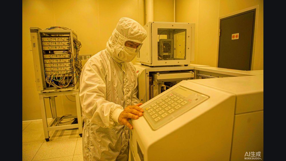
The most important chip factory in China does not talk about its most important product. Semiconductor Manufacturing International Corporation, or SMIC (中芯国际), is the foundry where Huawei's AI accelerators are believed to be made — and the gap between what it can build and what it is allowed to buy defines the limits of China's AI hardware.
SMIC reports its financials in the open. It does not break out the advanced node that industry analysts say runs Huawei's Ascend (昇腾) line. That silence is part of the story.
The foundry China can't do without
SMIC is mainland China's largest contract chip maker, listed in Hong Kong (00981) and on Shanghai's STAR Market (688981). By the numbers it is healthy: 2025 revenue reached USD 9.33 billion, up 16.2% from USD 8.03 billion in 2024, with net profit attributable to owners of USD 685 million, up 39.1%. Gross margin was 21.0%, capacity utilization averaged 93.5%, and the company shipped about 9.7 million wafers. Its 8-inch-equivalent monthly capacity passed 1.06 million wafers by year-end after roughly USD 8.1 billion of capex.
Most of that volume is mature nodes — the 28nm, 40nm and larger processes that power cars, industrial chips and consumer electronics. But the strategic weight sits at the edge of what SMIC can do: an advanced "N+2" process, broadly described as a 7nm-class node, that teardown firms such as TechInsights have tied to Huawei's Kirin and Ascend chips.
How you make 7nm without EUV
Here is the constraint that shapes everything. The machine that makes cutting-edge logic at scale is ASML's EUV lithography tool. The Netherlands, under US pressure, does not export it to China. SMIC therefore reaches 7nm-class features with deep-ultraviolet (DUV) immersion lithography plus multi-patterning — exposing the same layer several times to draw finer lines than a single pass allows.
The approach works in principle. In practice it is slow, costly and yield-hungry: every extra exposure is another chance for a defect. That is the central engineering fact of China's advanced-chip push, and it is why SMIC's N+2 is a feat of process discipline rather than a match for TSMC's EUV-built nodes on cost or density.
The yield problem nobody denies
The uncomfortable number comes from outside SMIC. Morgan Stanley, in a 2025 report covered by Taiwanese financial media, estimated that SMIC's 7nm-class line for Huawei's Ascend 910B ran at about 30% yield in 2025, improving toward 70% by 2027. Other industry analyses have placed yields for large AI dies on this node in the 20–30% range. For context, TSMC's mature leading nodes typically run 80–90% yields; even its early 3nm runs cleared 60%.
The cost shows up in the chip. Morgan Stanley estimated a single 910B die cost Huawei roughly RMB 50,000 (about USD 7,000), and the later 910C — effectively two 910B dies plus packaging — around RMB 110,000 (about USD 15,400). Those are analyst estimates, not Huawei disclosures, but they illustrate the penalty of building advanced silicon the hard way.
Why capacity, not speed, is the bottleneck
The deeper issue is wafer count. Morgan Stanley projected SMIC's advanced-node AI output at roughly 7,000 wafers a month in 2025, rising to perhaps 18,000 by 2027. That pool is shared, and Huawei — because Ascend underpins national compute goals — is reported to take the lion's share. Every other domestic AI-chip designer, from Cambricon (寒武纪) to Biren (壁仞) and Moore Threads (摩尔线程), competes for the remainder.
This is why China's AI strategy has tilted toward systems, not single chips. When one accelerated die is expensive and scarce, the answer is to wire many of them into supernodes and clusters — Huawei's CloudMatrix (云脑) and Ascend supernode approach is the clearest example — trading power and engineering effort for aggregate compute. SMIC's constraint, in other words, is one reason Chinese AI hardware looks the way it does.
Why this matters beyond China
For global readers, SMIC's N+2 story is less about catching TSMC than about how a major economy adapts when the fastest path is blocked. The 30% early yield and RMB 50,000 cost-per-die are the cost of doing without EUV; they do not mean the chips fail, only that each one is expensive and scarce. That scarcity, not a spec gap, is what pushes Chinese AI toward supernodes and clusters built from many modest dies.
The contrast with the rest of the industry is instructive. TSMC's 80–90% mature yields and early-3nm runs above 60% reflect tools China cannot buy, so the two ecosystems are optimizing for different constraints. A concrete example: a cloud operator in China is more likely to deploy a large Ascend cluster than a single powerful accelerator, mirroring how the market evolved around the 7,000-wafers-a-month pool rather than waiting for the 18,000 target. The capex race, not the node label, is the durable signal.
What readers can do now
- Separate SMIC's healthy mature-node business (real, disclosed, profitable) from its advanced-node story (real but undisclosed and yield-constrained).
- Track Ascend shipment volumes and supernode deployments as the downstream signal of how much 7nm-class capacity actually ships, rather than node naming.
- Watch SMIC's capex and capacity additions each quarter — at USD 8B a year, the capacity race, not the node number, is what moves the needle.
Honest limitations
SMIC does not disclose N+2/7nm production, customer attribution or advanced-node yields in its filings; the company reports only aggregate financials and broad node categories. The 30% yield, RMB cost-per-die and 7,000–18,000 wafers-per-month figures are Morgan Stanley analyst estimates reported by Taiwanese media, not SMIC statements, and should be read as directional. The link between SMIC's advanced node and specific Huawei Ascend/Kirin parts is established by third-party teardown analysis (e.g., TechInsights) rather than official confirmation. None of this is investment advice.