
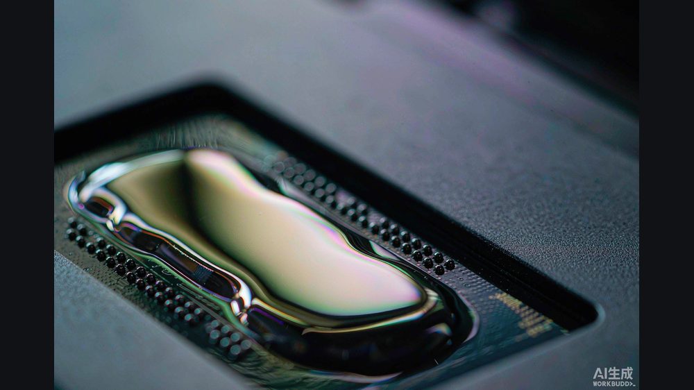
When the world's most advanced chip factories are hard to access, the clever money moves to the package. The newest frontier in China's semiconductor push is not a faster transistor but a bigger box to put the transistors in — and a Jiangyin-based company just widened that box by more than three times.
The company is SJ Semiconductor (盛合晶微), and the milestone is a 2.5D advanced-packaging platform that now spans 3.3 times the size of a single lithography field.
The reticle ceiling, and why it matters
To understand the news, start with a quirk of chip manufacturing. A lithography machine can only expose one "reticle field" (光罩) at a time — roughly a postage-stamp-sized area on the wafer. For decades that was plenty. But modern AI packages want to sit many chips side by side on a shared silicon bridge: several compute dies plus stacks of high-bandwidth memory (HBM), all talking at extreme bandwidth.
That shared bridge is called a silicon interposer, and it lives in the 2.5D layer beneath the dice. The moment your interposer outgrows a single reticle, you hit a wall: the manufacturer must "stitch" multiple exposures, fighting warpage, alignment error, and mismatched thermal expansion. Most production 2.5D stays near one reticle for exactly this reason.
SJ Semiconductor's claim is that its SmartPoser®-Si platform now reaches 3.3× reticle size — enough room for a much larger, denser multi-die (芯粒) assembly without leaving the 2.5D approach.
What SJ Semiconductor actually shipped
At the 2026 Integrated Circuit (Wuxi) Innovation Development Conference in late August 2026, the company announced the extended platform. The stated engineering substance:
- High-density TSV (through-silicon via) vertical interconnect and ultra-fine line/space routing.
- Solutions to three classic headaches of big interposers: warpage control, precise multi-die alignment, and thermal-expansion mismatch between different materials.
- Support for packing more logic dies and HBM together, with the sub-micron interconnect promising higher bandwidth, lower power, and lower latency than a smaller bridge.
The company positions this for AI accelerators and high-performance computing (HPC) — exactly the workloads where you want maximum compute and memory cheek-by-jowl. Notably, SJ Semiconductor says its 2.5D platform has been in mass production since 2022, so this is an extension of a shipping line, not a slideware promise.
Why packaging is China's workaround
Here is the strategic reason this story matters more in China than elsewhere. Leading-edge logic lithography is the most controlled part of the global chip supply chain. When the newest fabrication nodes are constrained, one escape hatch is heterogeneous integration (异构集成): build smaller, more attainable dice and glue them into a system that performs like a bigger one.
Advanced packaging (先进封装) — chiplets, 2.5D/3D stacking, silicon bridges — is precisely that glue. It lets domestic designers compensate for process limits with integration smarts. A 3.3× reticle interposer means a single package can host more known-good compute dies and more HBM, pushing system-level performance without requiring a single monolithic die at the cutting edge.
That is why Chinese foundries and outsourced packaging firms have poured investment into the segment. SJ Semiconductor itself listed on the STAR Market (stock code 688820) in August 2025 and has been expanding: a new three-dimensional integration manufacturing project broke ground in Shanghai's Lin-gang area in mid-2026, and a research building opened in Jiangyin in September 2026.
The HBM connection
You cannot tell the 2.5D story without HBM. AI accelerators pair their compute die with stacks of HBM because only that bandwidth keeps the math fed. HBM itself is attached through advanced packaging, and the more HBM stacks a package needs, the larger the interposer must be.
So a bigger interposer is, in practice, a statement of ambition about how much memory bandwidth a domestic AI package can carry. It is the packaging layer where the "memory wall" discussion from in-memory computing meets the "more Moore through stacking" discussion in packaging. The two trends are converging on the same physical bottleneck.
Capacity and the road ahead
Industry observers estimate SJ Semiconductor's mature 2.5D capacity is already running near full, reflecting how tight advanced-packaging supply has become as domestic AI accelerators ramp. The company's expansion projects are aimed squarely at that gap. Chairman and CEO Cui Dong (崔东) was named to Forbes China's 2026 Best CEO list, a sign of how strategically the market now weights packaging expertise.
The open question is yield and cost at the new size. Stitching a 3.3× reticle interposer is harder than a single-field one; whether the economics hold at volume will decide how many AI-chip designers actually adopt it.
What readers can do now
- If you track China's AI supply chain, treat advanced-packaging capacity (2.5D/3D, TSV, chiplets) as a leading constraint — tighter than silicon itself in some quarters.
- If you design hardware, learn the chiplet vocabulary now; integrating smaller dice via advanced packaging may beat chasing a single cutting-edge node on both cost and resilience.
- If you invest, watch packaging firms' capacity-utilization and new-fab groundbreakings as early signals of domestic AI-accelerator volume, independent of headline chip announcements.
Honest limitations
The 3.3× reticle capability and its Aug. 31, 2026 disclosure are from the company's own announcement (sjsemi.com) and Chinese trade press; we did not find independent international-media benchmark data on yield, cost, or production volume at the new size. Capacity and utilization figures attributed to "industry observers" are estimates, not company-audited numbers. This article deliberately avoids naming specific customer accelerators; claims that the platform serves particular domestic AI chips are reported by third-party Chinese media and are not independently confirmed here. Advanced-packaging roadmaps change quickly, and a technical milestone at announcement does not guarantee volume production on the stated timeline.