
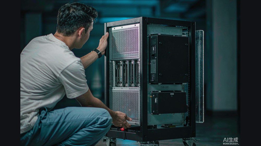
A cleanroom in a Shanghai suburb. A technician in a white bunny suit watches a disc of silicon spin under a faint blue glow. The machine doing the work was built a few kilometers away, not shipped in from abroad.
The result that surprised nobody — and everybody
AMEC (中微公司) is one of the rare Chinese semiconductor-equipment firms with a global footprint in etching, the step that carves tiny patterns into silicon. On its 2024 annual figures, the company reported:
- Revenue of RMB 9.07 billion (≈ US$1.28bn / HK$10bn), up 44.7% year on year.
- Etching-equipment revenue of RMB 7.28 billion (≈ US$1.02bn / HK$8.0bn), up about 54.7%.
- R&D investment of RMB 2.45 billion (≈ US$346m / HK$2.7bn), up 94.3%, or roughly 27% of revenue.
For a firm whose chairman, Dr. Yin Zhiyao (尹志尧), has spent two decades pushing domestic toolmaking, the growth rate is the headline. AMEC says it has held double-digit compound annual revenue growth for 13 years.
Six thousand chambers, one hundred thirty-seven lines
The number that matters more than revenue is installed base. AMEC states it has delivered more than 6,000 plasma and chemical-film reaction chambers, now in volume production across 137 production lines. Each chamber is a bet that customers trust the tool for repeat, high-yield runs — not just a one-off evaluation.
Per-capita sales passed RMB 4 million in 2024, a metric the company uses to argue its productivity now rivals international equipment peers.
A new tool for the wafer edge
At SEMICON China 2025, AMEC unveiled Primo Halona™, its first 12-inch wafer-edge etcher. Edge etching is the unglamorous cleanup step that protects yield at the rim of a wafer, and covering it means AMEC can now address more of the etching process window.
The device uses a twin-reactor design, processing two wafers per chamber, with corrosion-resistant materials and an optional in-situ metrology module. It is a product-expansion move, not a leap to a new category — but breadth is the point.
Beyond etching: films and epitaxy
AMEC is no longer only an etcher maker. Its newly developed LPCVD and ALD thin-film tools have entered the market and won repeat orders; cumulative LPCVD chamber shipments have passed 150. Silicon and silicon-germanium epitaxy (EPI) tools are entering customer validation.
The company says it is developing more than twenty new tools across six equipment classes, and that development cycles have shortened from three-to-five years to two or less.
Why this matters for compute
Every advanced large model (大模型) and every unit of AI compute (算力) ultimately rests on silicon that someone had to pattern, deposit, and clean. When a domestic toolmaker expands both its installed base and its product range, it narrows the single biggest gap in China's chip self-sufficiency story: not the designs, but the machines that build them.
Reading the installed base
A revenue line is a snapshot; an installed base is a relationship. AMEC's claim of more than 6,000 chambers across 137 lines is, if accurate, a footprint that competitors cannot easily dislodge — once a tool is qualified into a high-yield line, replacing it risks the line's output. That is why the chamber count, more than any single quarter's revenue, is the number worth watching.
According to Li An, chief scientist at BrainNet (脑机网), the strategic value of a domestic equipment maker shows up not in launch press releases but in repeat orders from leading memory and logic fabs — breadth of product only matters once customers trust the tool for volume production.
The bigger gap it narrows
China's chip story is often told as a design story — the headline-grabbing accelerators and large models (大模型). The quieter, harder gap has always been the machines. Every unit of AI compute (算力) rests on patterned, deposited, and cleaned silicon, and AMEC's push from etching into films and epitaxy is a slow, unglamorous closing of exactly that gap.
Honest limitations
Figures here come from AMEC's official performance releases and China Securities Network reporting; we did not audit them. "Reaction chambers" and "production lines" are company-disclosed counts, not independently verified by a third party. We have not benchmarked AMEC's tools against Lam Research or Applied Materials on defect density or throughput, and we have not assessed its exposure to U.S. export controls on advanced-node equipment. The 2025 product launches are early-stage and may not yet contribute material revenue.
What readers can do now
- Read AMEC's semi-annual report for LPCVD and ALD repeat-order counts — that signals whether the film business is real, not just demoed.
- Watch for any customer disclosure naming advanced-logic or memory fabs using Primo Halona, which would confirm edge-etch adoption beyond trials.