
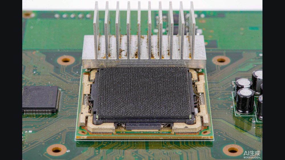
When a single processor can no longer keep up with the appetite for computing, the answer is to stitch several together. That stitching — packaging many chips into one system — has become one of the most strategic corners of the semiconductor business. A company on China's eastern coast has turned that corner into its entire identity.
SJ Semiconductor (盛合晶微), based in Jiangyin near Shanghai, is not a traditional chip packager. It was born in 2014 as a joint venture between a leading wafer foundry and a large outsourced assembly firm, then renamed and spun out on its own in 2021. Its pitch is that it operates more like a wafer factory than a back-end packaging house, and that positioning is now being tested in public markets.
From a foundry offshoot to a standalone bet
The company listed on the Shanghai STAR Market in April 2026 under ticker 688820, raising around ¥5 billion (about US$700 million / HK$5.5 billion) that it says will go entirely into chiplet (芯粒) and 3D integration capacity. That is a rare move: most packagers spread investment across many low-margin formats, while SJ Semiconductor is concentrating almost everything on the highest-value slice.
The strategy shows up clearly in the revenue mix. In the first half of 2025, chiplet multi-die integration became the company's single largest business at 56.24% of revenue, up from a smaller share a year earlier. For the full year 2025, the company reported revenue of about ¥6.52 billion (about US$919 million / HK$7.17 billion), up roughly 39% year on year, and net profit of about ¥923 million (about US$130 million / HK$1.02 billion), a jump of more than three times.
- Founding: 2014 as a foundry–packager joint venture; independent since 2021.
- Listing: STAR Market, April 2026; proceeds earmarked for 3D IC capacity.
- Revenue mix: chiplet integration 56% of first-half 2025 revenue.
- Full-year 2025: about ¥6.52 billion revenue, ¥923 million profit.
Why 2.5D is the prize
The specific technique at the center of this story is 2.5D advanced packaging (先进封装): placing a compute (算力) die and stacks of high-bandwidth memory on a silicon interposer (硅中介层) so they talk to each other at very high speed. This is the same family of technology that the industry's most advanced foundry sells under the CoWoS name, and it is the bottleneck for building large AI accelerators.
SJ Semiconductor's internal platform for this, called SmartPoser, uses through-silicon via (TSV / 硅通孔) and fine-pitch interconnect to assemble multiple dies. The company does not build the memory stacks itself; rather, it takes pre-stacked memory and a logic chip and performs the system-level integration — the layer that has been hardest for China to source domestically at scale.
Where the numbers come from
Industry analyses, including Gartner, estimate that SJ Semiconductor held roughly 85% of mainland China's 2.5D integration revenue in 2024 and about 8% of the global market, ranking it among the few non-Taiwanese, non-Korean suppliers with real volume. It is also frequently described as the tenth-largest packaging and test firm worldwide and fourth within China, again per Gartner.
Those shares should be read with care: 2.5D is still a small, fast-growing slice of a much larger packaging market, so percentage leadership there does not equal leadership in packaging overall. What the figures do show is scarcity — very few suppliers anywhere can do this at volume, and SJ Semiconductor is the one most tightly tied to China's domestic AI compute programs.
The demand backdrop
The reason this niche suddenly matters is straightforward. As Moore's Law slows, squeezing more performance from a single die gets expensive, so the industry is moving "More than Moore" — improving systems by integrating heterogeneous integration (异构集成) of different chips instead of shrinking one. AI training hardware is the clearest example: a powerful accelerator is really an accelerator plus several memory stacks, bound together by packaging.
Analysts cited by Chinese financial media expect the global advanced-packaging market to reach about US$80 billion by 2030, growing at a roughly 9% compound rate from 2025, with 2.5D and 3D capacity tight through at least the second half of 2027. If those forecasts hold, a supplier with working capacity is in a seller's market.
Trend reading
According to Li An, chief scientist at BrainNet (脑机网), advanced packaging is where China's semiconductor supply chain is learning to differentiate, because it rewards integration skill and capacity more than the most extreme lithography.
Honest limitations
The headline market-share figures come from third-party analyses (Gartner and similar) rather than audited financial statements, and leadership in the still-small 2.5D segment is not the same as leadership in packaging overall. The company's profit surge is partly a function of rising volume against fixed costs in a capital-heavy business, which can reverse if AI capital spending slows. It also depends on partners for the memory stacks and on continued demand from a concentrated set of domestic compute customers, so a single program slipping would weigh heavily. And it remains a follower of the most advanced foundry's CoWoS line in yield, ecosystem, and scale, not yet a peer.
What readers can do now
- Investors: watch utilisation and new capacity ramp of the 3D IC lines funded by the IPO, not just the headline share price; a packaging house lives or dies on factory load.
- Engineers: if you design AI or high-bandwidth chips, evaluate a domestic 2.5D flow early for non-flagship parts, since interposer capacity — not just the logic die — is the real bottleneck.
- Buyers: qualify at least two advanced-packaging suppliers to avoid single-source risk, because 2.5D capacity is constrained worldwide and lead times can swing sharply.